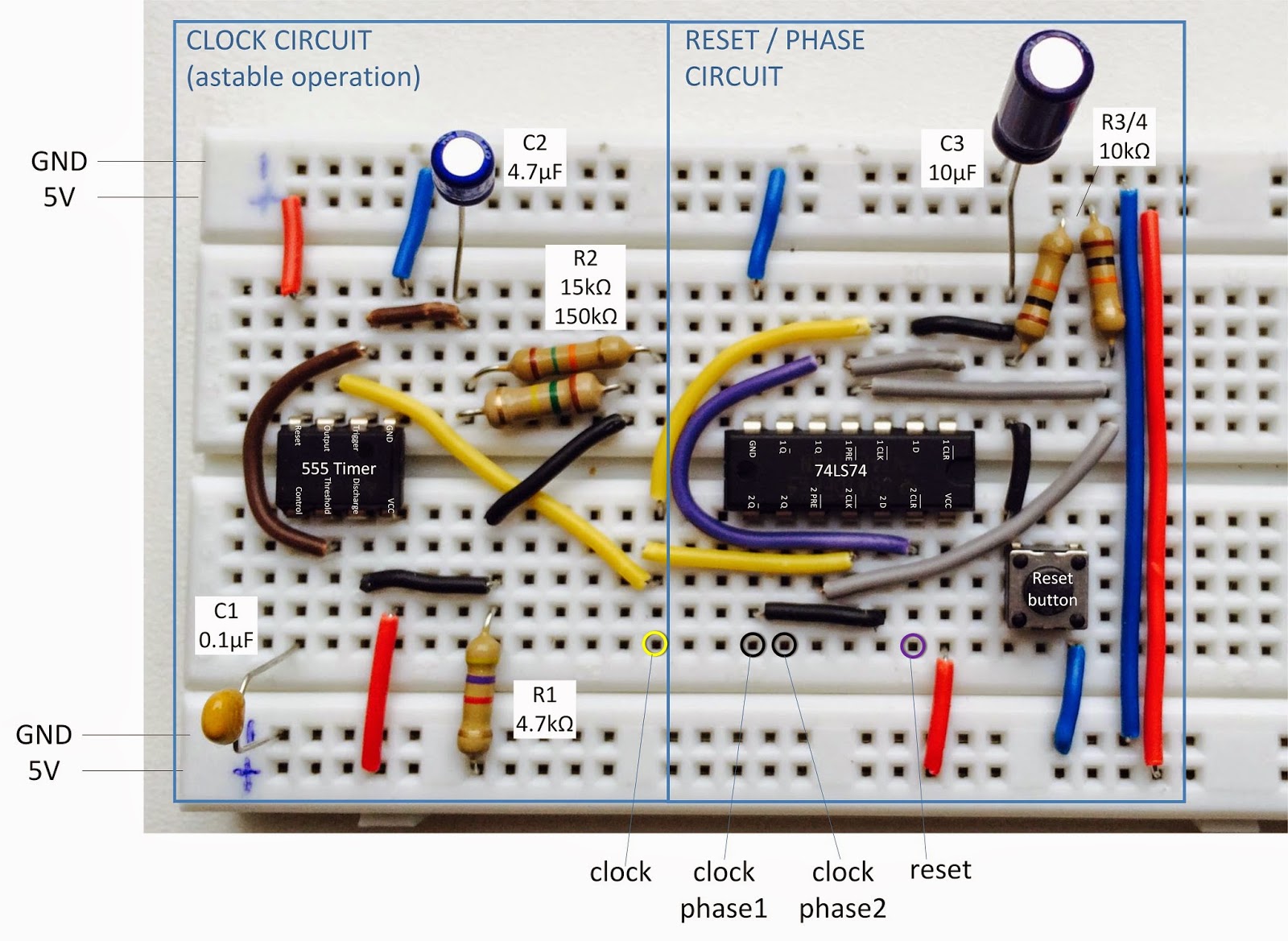
The Clock, Phase and Reset circuit
The clock circuit is based on the 555 Timer chip. In the configuration above it outputs a 1 Hz clock signal on the ouput labelled with 'clock' (yellow). Slow, but great for debugging purposes.
 |
| Source http://www.555-timer-circuits.com/operating-modes.html |
The computer will work with a fetch instruction (phase 1) & execute instruction (phase 2) each taking 1 clock cycle. The second flipflop on the 7474 is used to divide the clock signal into the two phases needed.
The first flipflop on the 7474 is used in the Power-on-reset circuit. When the power is switched on, capacitor C3 will charge and during the time it is below 0.8V (logic LOW), it will output a logic LOW on the output labelled 'reset' (purple). When the capacitor is charged enough, a logic HIGH will be put on the reset output.
So the computer is in the RESET state when a logic LOW is put on the reset output. The phase 1 output will be kept LOW while in the RESET state.The reset button will decharge the capacitor while pushed putting the computer in a RESET state again. When released, it will follow the power on sequence as described above.
Outstanding Questions:
Outstanding Questions:
- what happens when the voltage of input 1D is in the undefined logic level region when the capacitor is charging and the clock signal goes from LOW to HIGH? Should I use a Smitt Trigger in stead?
- What capacitor value should I use for the 555 Timer control voltage? Currently I used 0.1uF. Need to switch to the recommended 0.01uF.
- Do the capacitors discharge when the power is removed?
The following video shows the circuit in action. The four LEDs show the clock, phase1, phase2 and reset signal from left to right.
Geen opmerkingen:
Een reactie posten