zondag 16 november 2014

EEPROM programmer using Arduino

Introduction

Don't want to pay a lot of money for an EEPROM programmer? Build it yourself using an Arduino!

So what components do you need to build a programmer for 8KB EEPROMs (type 28C64):
  • a breadboard (830 pins)
  • ZIF Socket (28 pin) to hold the EEPROM
  • 2x 74HC595 8-bit shift register
  • 2x 10Kohm resistor
  • an Arduino 
  • wires (different colors)
  • USB cable to connect the programmer to a PC
  • a program for the Arduino
  • a client program for reading, and one for writing
All project files can be found in this online folder.

What I would like to achieve is that a binary file (8KB or less) on a client, in my case a Windows 7 laptop, is programmed into the EEPROM with a single command. 
Also, with a single command, I would like to copy the entire contents of the EEPROM in a binary file on the client.
So how does it work?

The arduino is running a program that listens to the serial port, waiting for 2 commands: Write to EEPROM and read from EEPROM 


For the (windows) client, I wrote two PowerShell scripts, one for reading


and one for writing


The read script receives a continuous stream of all 8192 bytes from the Arduino and store it into the specified file.

The write script sends the input file in blocks of 1024 bytes to the Arduino (due to RAM limitations on the Arduino) and waits for the signal that all bytes are programmed into the EEPROM.

Design

The schematic below shows how the different components should be wired.


Build


Future work:

  • The EEPROM programmer that I describe above is fully functional, but programming could be made a lot faster. The EEPROM programming cycle takes 5ms and currently this is done per byte. The EEPROM can also do 'page writing' where 64 bytes are programmed in a single cycle.
  • Soldering the circuit on a protype board.


woensdag 5 november 2014

The Build

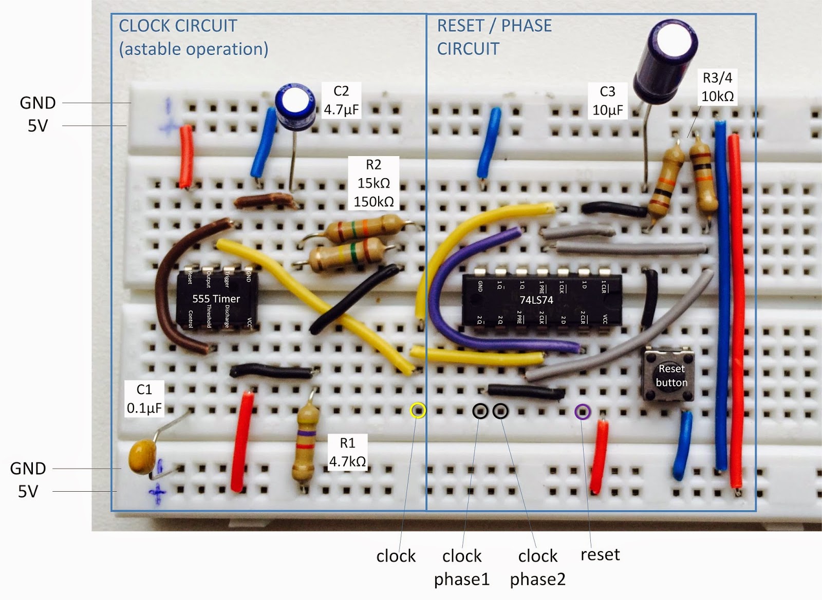
The Clock, Phase and Reset circuit


The clock circuit is based on the 555 Timer chip. In the configuration above it outputs a 1 Hz clock signal on the ouput labelled with 'clock' (yellow). Slow, but great for debugging purposes.


Source http://www.555-timer-circuits.com/operating-modes.html
The computer will work with a fetch instruction (phase 1) & execute instruction (phase 2) each taking 1 clock cycle. The second flipflop on the 7474 is used to divide the clock signal into the two phases needed. 

The first flipflop on the 7474 is used in the Power-on-reset circuit. When the power is switched on, capacitor C3 will charge and during the time it is below 0.8V (logic LOW), it will output a  logic LOW on the output labelled 'reset' (purple). When the capacitor is charged enough, a logic HIGH will be put on the reset output. 

So the computer is in the RESET state when a logic LOW is put on the reset output. The phase 1 output will be kept LOW while in the RESET state.The reset button will decharge the capacitor while pushed putting the computer in a RESET state again. When released, it will follow the power on sequence as described above.

Outstanding Questions: 
  • what happens when the voltage of input 1D is in the undefined logic level region when the capacitor is charging and the clock signal goes from LOW to HIGH? Should I use a Smitt Trigger in stead?
  • What capacitor value should I use for the 555 Timer control voltage? Currently I used 0.1uF. Need to switch to the recommended 0.01uF.
  • Do the capacitors discharge when the power is removed?

The following video shows the circuit in action. The four LEDs show the clock, phase1, phase2 and reset signal from left to right.


The Design

Paul's Digital Computer

A few weeks ago, I got this crazy idea to build a CPU from scratch without using a micro processor, but construct it entirely from discrete logic circuits. I have chosen to use TTL ICs to implement the logic and CMOS technology for memory. With Google as my best friend to start off with, I came across many similar DIY projects. The Nibbler project got my attention and confirmed that my initial thought on finishing such a build would be feasible.

My goal was not to come up with an entirely new design, but create it from scratch and understand every single bit of the design. I will call it the PDC-1 which stands for Paul's first Digital Computer and are also my initials :-)

I created the entire circuit in Proteus 8 that can also simulate the entire circuit.


The high level requirements
  • real 4-bit processing: the ALU and databus are 4-bits
  • harvard architecture: program and data in separate memory
  • 12-bit memory addressing (32kbit RAM; 4096 x 8-bit)
  • instruction set contains 16 instructions
  • microcode for instructions stored in 2 EEPROMS
  • 2x 4-bit input and 2x 4-bit output
  • only 1 register, the Accumulator